In order to obtain gm value of a mos for hand calculations of capacitance etc,
1) Perform dc analysis ( simple dc analysis).
2) Use " direct plot " if the conventional method of dc analysis takes too much time (as it did in my case).
3) Analog simulation envt->results
4) Select the option that gives you transistor parameters
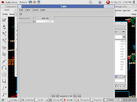
4) Right click on gm. Select table and you will obtain the gm of the desired mosfet :)
Friday, April 17, 2009
Design of a 2 stage op amp
DESIGN CONSTRAINTS:
1)SR = 10 V/usec
2)Av = 5000 V/V
3)GB = 5 MHz
4)CL = 100 fF
5)Pdiss < 0.3 mWatt
6)ICMR+ = 1.5 Volt
7)ICMR- = 0.2 Volt
Design consideration:
We consider that
1)10uA current flows through 1st stage
2)20uA current flows through the next stage
3)A cascoded current mirror it used for realizing the current source( vary its W/L to get 20uA and 10uA currents resp).
TECHNOLOGY USED: 180nm technology corresponding AC analysis gives:
This is the Mag-Phase plot for (0-10^12)Hz frequency range.
Problems Encountered:
1) Regarding phase plot:
Between (10^8- 10^9),in the magnitude curve, we have a - 40dB slope(due to presence of poles) .There after we have a zero. So theoretically there should be a positive slope for the phase plot (due to the presence of zero), though no such thing can be observed from the simulation result.
2) Regarding frequency compensation:
Variation in R and Cc is not giving much difference in the frequency response (phase margin).
Monday, April 6, 2009
UTube Ripper in Ubuntu
1) Download .deb package from here
2)After downloading Double click the file to start installation. This will fetch and install all its dependencies.
3)Go to Applications—>Internet—>Utube-ripper
Sunday, April 5, 2009
MUST SEE links on Electronics
1)Lectures by Jacob Baker
2)Videos on CMOS
3)MIT video lectures on circuits and electronics
4)MIT Course material on analysis and design of Digtal ICs
5)MIT Course material on Microelecronics devices and circuits-I
6)MIT Course material on Microelecronics devices and circuits-II 7)Principles of digital communication - I(video)
8)Principles of digital communication - II(video)
9)High speed communication circuits
Saturday, March 28, 2009
high "OCTAVE"
GNU OCTAVE is a powerful tool on Linux which is similar to MATLAB for Windows. The syntax is almost the same.
It is easy to install.
The installation can be done as:
system -> Administration -> synaptic packet manager
select octave3 from the package and install it.
We have already obtained a set of data obtained from gmid.dat (refer to the prev post).Open it with openoffice. At the right end of openoffice there is an option "std",click it thrice to get "blk".By selecting blk, we can select the data columnwise,(which isn't possible otherwise).
Open up a terminal.
Type octave
octave:1>gm = [ gm values copied from the gmid.dat]
//press q to escape the END statement
octave:2>id = [ id values copied from the gmid.dat]
octave:3>plot (gm,id)
octave:4>xlabel('gm')
octave:5>ylabel('id)
octave:6>title('gm vs id curve')
to save the plot, go back to the terminal,
octave:7>print("figure1.png")
octave:8>reload
Friday, March 27, 2009
gm/Id plot in cadence
Our main concern is to get suitable method for determining the size of the transistors for any region of operation.We know that the old transistor design equations are no longer sufficient enough for the design of any circuit in submicron region due to various other iterative parameters that come in picture.So to design a circuit we select the sizes from our old experience and then try to optimize it. This approach is very tedious.
In this project thus we try to find out the design parameters in submicron regime, using a plot between gm/id and id/(w/l).
In order to obtain a Gm/Id plot in cadence(for 180um technology),the following steps are to be done:
1) create a simple nmos ckt, with Vgs and Gdd set to 1.8V
2)As spectre doesnt save the DC operating point, so we can save them by the following steps:
a)change simulator to spectre
b)create info.scs file from text editor and save it in the folder which contains all other files of cadence
c) write in the info.scs file:
save N0:oppoint
d)(here N0 is the instance name for the NMOS used in the circuit).Add info.scs as model library in through analog environment.
e)select AWD waveform tool.This can be done by:
Analog Environment -> options -> select waveform tools : AWD
f)sweep Vgs from 0 to 1.8V using DC analysis.
g)Run simulation and go to the result browser as:
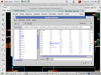
Analog design Environment-> tools -> result browser
then
schematic->psf/ -> Run 1 -> DC to DC -> N0
this gives the see DC operating points saved
h)Right click Gm and get the gm plot
3)We used OCEAN to get the desired curves then
4)Analog Environment -> menu -> save script
this script file gives us the setup we have made for simulation
5)Add few lines to this simple script file to save the DC operating point parameters you are
interested in (copy this text exactly):
selectResult('dc)
plot(getData("N0:gm"))
ocnPrint(?output "~/gmid.dat" ?numberNotation 'scientific
getData("N0:gm"),getData("N0:id"))
6)Load this file and run the simulation again from CIW window by typing:
load(“gmid.ocn”)
7)Go to the root directory (or where ever you saved the file) and you can find gmid.dat. All the desired parameters gm, Id are saved here.
Design of a simple Constant Current Source Circuit in Cadence Viruoso:
A simple current source can be realized by using a current mirror circuit.
A current mirror consists of 2 NMOS (M1 and M2) placed back to back the drain gate terminal connected for M1. This provides a feedback path to the current and thus keeps the current in M1 constant.
A resistance R1 is connected between the drain of M1 and VDD. We fix the value of primary current (input current ) by adjusting the value of R1.
So for a given inpur current I,
R1(approx)= (VDD-Vgs)/I
Once R1 is determined, Connect the drain terminal of M2 to a voltage source V2 and sweep it from 0 to 1.8V (using DC analysis , for 1.8um technology).
Plot the graph of Vgs vs V2 and determine the region where saturation occurs.
Now keeping the value of V2 in the region such that all the transistors are in saturation, vary the W/L of the MOSFETs.
It will be found that in such case our current through M2 will be directly proportional to the (W/L)of M2 wrt W/L of N1.
keeping the W/L of M1 fixed , vary the W/L of M2. The current through M2 will also vary in the same manner.
I1/I2 = (W/L)1/(W/L)2
It should be noted that theres a particular current range for which this relation holds good and it doesn't beyond this range.
APPLICATION OF A CURRENT SOURCE IN A SIMPLE TWO STAGE OP AMP (designed using 0.18um technology)
here we have used a cascoded current mirror as current source.
Subscribe to:
Posts (Atom)